


Revolutionary Applications of Ceramic 3D Printing in Advanced Electronic Devices
Release time:
2025-07-24
Introduction: When Additive Manufacturing Meets the Electronics Industry
Additive Manufacturing (AM), also known as 3D printing technology, is rapidly transitioning from laboratory prototyping to industrial-scale production, with its influence permeating various high-value fields such as aerospace, medical, and automotive industries. According to Protolabs' "2024 3D Printing Trends Report," the global 3D printing market size is expected to reach $57.1 billion by 2028. Simultaneously, VoxelMatters' market report indicates that the number of 3D-printed components in the consumer electronics sector increased by 23% year-on-year in 2023. These data suggest that additive manufacturing is increasingly becoming a core force driving manufacturing transformation, used for producing final functional parts.
However, the rapidly developing electronics industry, driven by Moore's Law, faces severe challenges. As devices miniaturize and functional integration increases, traditional subtractive manufacturing (e.g., CNC machining) proves inadequate in handling complex geometric structures, high-density integrated heat dissipation, and multi-material integration. Building precise internal channels at micro- or even nano-scales, achieving efficient heat dissipation, and seamlessly integrating materials with different properties have become key bottlenecks restricting the development of next-generation electronic products.
Additive manufacturing, with its unique "layer-by-layer" approach, offers disruptive ideas for solving these problems, giving engineers unprecedented design freedom to create complex structures unattainable with traditional processes. This article will focus on a highly promising and crucial sub-field within additive manufacturing technology—the additive manufacturing of ceramic materials—and delve into how it plays a revolutionary role in the development of advanced electronic devices.
Among various 3D printing technologies, photocuring technology, especially Digital Light Processing (DLP), stands out in the manufacturing of precision ceramic components due to its excellent printing accuracy and efficiency. DLP technology prepares a slurry by mixing ceramic powder with photosensitive resin, enabling layer-by-layer curing with extremely high resolution, laying a solid foundation for manufacturing miniaturized, high-precision electronic components. Next, we will deeply analyze the core advantages of ceramic 3D printing and, through a series of cutting-edge application cases, reveal how this technology is reshaping the future of the electronics industry.
Core Advantages: Why Choose Ceramics for 3D Printing?
In electronic applications, material selection is crucial, directly determining device performance, reliability, and lifespan. Ceramic materials such as alumina, aluminum nitride, and silicon carbide have long been favored for their excellent comprehensive properties. However, their broad application has been limited by traditional processing techniques. The emergence of additive manufacturing provides the key to unleashing the full potential of ceramics.
Inherent Value of Ceramics: The Ideal "Skeleton" for Electronic Devices
Ceramic materials hold irreplaceable value in the electronics field, stemming from their multifaceted excellent properties:
Excellent Electrical Properties: Ceramics are excellent electrical insulators, effectively preventing current leakage and signal crosstalk, serving as the cornerstone for ensuring signal integrity in chip packaging and high-frequency circuits.
Unique Thermal Properties: Ceramics typically have low thermal conductivity, making them ideal thermal insulation materials. Their coefficient of thermal expansion (CTE) is generally low and highly compatible with semiconductor materials like silicon. This ensures minimal thermal stress between the ceramic substrate and the chip during drastic temperature changes in electronic devices, thereby ensuring the long-term reliability of internal microscopic structures and electrical connections, significantly reducing the risk of failure due to thermal mismatch.
Outstanding Mechanical and Chemical Stability: Ceramic materials possess high mechanical strength, high hardness, wear resistance, and excellent chemical corrosion resistance. This allows ceramic-based electronic components to operate stably for extended periods in harsh environments such as high temperature, high humidity, and corrosive gases, meeting the extreme requirements of industrial, automotive, and aerospace fields.
Bottlenecks of Traditional Manufacturing: The "Soft Underbelly" of Hard Materials
Despite their superior performance, the "hard" and "brittle" physical properties of ceramics pose significant processing challenges. Traditional subtractive manufacturing methods, such as cutting, drilling, and grinding, face numerous difficulties when processing ceramics:
High Processing Difficulty and Cost: High hardness leads to severe tool wear, low processing efficiency, and high costs.
Limited Design Freedom: Brittleness makes it difficult to process ceramics into structures with complex internal channels, intricate networks, or thin walls, greatly limiting engineers' design imagination.
Miniaturization Challenges: Manufacturing precise ceramic structures at the micron level is almost impossible with traditional processes, posing an obstacle to the development of microelectronics and micro-electromechanical systems (MEMS).
Additive Manufacturing's Breakthrough: Giving Ceramics Infinite Forms
Photocuring 3D printing technology, especially DLP, has brought a revolutionary breakthrough to ceramic forming. Its process cleverly circumvents the difficulties of traditional processing:
Slurry Preparation: Micron or nano-sized ceramic powders are uniformly mixed with a specially formulated photosensitive resin to form a ceramic slurry with good fluidity and photosensitive properties.
Photocuring Forming: The slurry is placed in a printing device, and the DLP system selectively cures the slurry layer by layer by projecting specific patterns of ultraviolet light according to the digital model. Unexposed slurry remains liquid, providing support for the next layer. This process can build complex geometric shapes with extremely high precision, forming what is known as a "Green Part".
Post-processing: The printed green part undergoes two critical post-processing steps: debinding and sintering. Debinding removes the photosensitive resin matrix from the part through gentle heating; sintering then fuses and densifies ceramic particles at high temperatures (usually over 1000°C), ultimately forming a strong, pure ceramic part.
Through this process, additive manufacturing not only fully preserves the inherent excellent physical and chemical properties of ceramic materials but, more importantly, it breaks the form constraints of traditional processes, giving ceramics almost infinite design freedom. This makes it possible to manufacture ceramic electronic components with complex internal cooling channels, lightweight lattice structures, and highly integrated functions.
Disruptive Applications: Practical Cases of Ceramic 3D Printing
Ceramic 3D printing technology has demonstrated disruptive potential in several cutting-edge electronic applications. The following three cases, from precision instruments to functional materials and advanced packaging, clearly show how this technology solves core industry pain points and creates new possibilities.
Case 1: Miniaturization Revolution in Precision Instruments – Quantum Frequency Reference Devices
Application Scenario: Manufacturing compact quantum frequency reference devices for high-precision fields such as Global Positioning Systems (GPS), deep space navigation, precise timing, and secure communication.
Core Challenge: These devices traditionally rely on large and complex optical platforms, with miniaturization and integration being key bottlenecks for achieving portable applications and space deployment.
Solution: Utilizing Lithoz's commercialized DLP ceramic 3D printing technology, a miniature optical bench integrating complex optical component (e.g., lenses, prisms) fixing structures and gas chambers was successfully printed using highly stable alumina as the material.
In this case, alumina ceramic provided excellent dimensional stability and low thermal expansion characteristics, ensuring the positional accuracy of optical components under temperature fluctuations. 3D printing technology made it possible to integrate multiple separate components, which traditionally required precision assembly, into a single, structurally complex miniature platform. This not only significantly reduced the device volume, from "desktop-sized" to "chip-sized," but also remarkably improved its vibration and shock resistance. This breakthrough strongly proves that ceramic 3D printing is a key enabling technology for the miniaturization and robustness of high-end precision instruments, and it also opens up broad prospects for the development of miniature sensors, space probes, and portable medical diagnostic devices.
Case 2: On-demand Customization of Functional Materials – Conductive Ceramic Composites
Application Scenario: Developing a new functional material that simultaneously possesses good electrical conductivity (for circuits or electrothermal components) and low thermal conductivity (for thermal insulation or thermal management), and can operate stably at temperatures up to 600°C.
Core Challenge: Electrical conductivity and thermal insulation are typically contradictory in traditional materials. Metals have good electrical conductivity but also high thermal conductivity, while traditional ceramics have good thermal insulation but are insulators.
Solution: Through 3D printing, graphene nanosheets were uniformly dispersed as conductive fillers and cured in a silicon carbide ceramic matrix, forming a new ceramic-graphene composite material.
The significance of this case goes beyond mere "forming," marking the entry of additive manufacturing into a new phase of "Material Creation". By precisely controlling the concentration and distribution of graphene within the ceramic matrix, researchers can "customize" the material's electrical conductivity on demand, while retaining the excellent high-temperature resistance and low thermal conductivity of silicon carbide ceramic. Compared to metals, this composite material has lower density and more stable high-temperature resistivity, offering new material options for designing novel heating elements, high-temperature sensors, and thermoelectric devices. 3D printing plays an indispensable role in this process, ensuring the uniform mixing and precise forming of nano-functional fillers in the matrix, which is difficult to achieve with traditional powder metallurgy or sintering processes. This demonstrates the immense potential of additive manufacturing in developing new composite materials with specific, even programmable functions.
Case 3: "Interchanges" for Advanced Packaging – 3D Interconnect Technology
Application Scenario: Providing ceramic interposers for 3D vertical integration required by high-performance chips such as Graphics Processing Units (GPUs) and High-Bandwidth Memory (HBM).
Core Challenge: As chip design shifts from traditional 2D planar layouts to more efficient 3D vertical stacking (Chiplet), thousands of high-density electrical interconnect channels (Vias) need to be built in extremely small spaces to connect upper and lower chips. Traditional methods can only produce straight vertical channels, limiting wiring density, signal path optimization, and heat dissipation design.
Solution: Using ultra-high resolution photocuring 3D printing technology from companies like Boston Micro Fabrication, ceramic interposers with curved, non-planar electrical channels were manufactured using amorphous silicon dioxide as the base material, with the finest feature sizes reaching the 10-micron level.
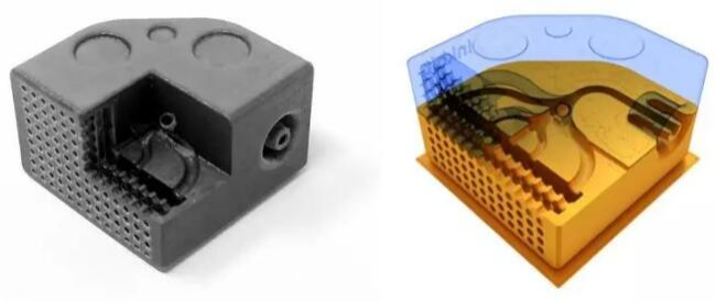
This represents a disruptive breakthrough in traditional semiconductor packaging technology. The 3D-printed ceramic interposer is like building a complex interchange and tunnel system for "electronic traffic" inside the chip. These curved channels can achieve shorter signal paths, increase interconnect density, and optimize heat dissipation and mechanical performance. This case clearly demonstrates that ceramic 3D printing technology is not just a manufacturing tool but a core enabling technology driving the development of next-generation high-performance computing, artificial intelligence chips, and advanced sensors. It is building the crucial physical foundation for the "More than Moore" era.
Challenges and Outlook: The Path to the Future
Despite the immense application potential demonstrated by ceramic 3D printing technology, a series of challenges still need to be overcome to achieve a leap from cutting-edge research to widespread industrial application. At the same time, technological integration and innovation also paint an exciting blueprint for its future development.
Key Points: Addressing Current Challenges
Material Bottlenecks: The variety of high-performance, high-stability ceramic photosensitive resins (slurries) is still limited, especially in multi-material printing. Material cost, batch stability, and compatibility with the printing process are key factors restricting its large-scale application.
Process Complexity: Post-processing, especially debinding and sintering, is crucial for the final product's accuracy and performance. Volume shrinkage and potential deformation during sintering require precise control, necessitating deep process knowledge and accumulated experience. Furthermore, the interfacial bonding strength between different materials in multi-material printing is a significant technical challenge.
Lack of Standardization: Currently, there is a lack of unified standardization systems for material performance, process flow, and final component quality inspection within the industry. This lack of standards hinders the reliability verification of the technology and its widespread adoption in critical fields.
Equipment and Cost: High-precision ceramic 3D printing equipment, especially systems capable of achieving micron-level resolution, involves high initial investment costs. Simultaneously, the complexity of the entire process chain (from slurry preparation to post-processing) also leads to higher operating costs.
Future Outlook: Evolution Driven by Integration and Intelligence
Facing these challenges, academia and industry are actively exploring solutions, and future development will primarily focus on the following directions:
Multi-material and Functional Integration: The future trend will be to move from printing single-function structural parts to directly printing "smart devices" integrating conductive paths, insulating layers, sensing elements, heat dissipation structures, and even microfluidic channels. This will greatly simplify electronic product assembly processes and achieve unprecedented functional integration.
Artificial Intelligence (AI) Empowerment: AI will play an increasingly important role in ceramic additive manufacturing. For example, AI can be used for topology optimization design to generate the lightest and most efficient structures while meeting performance requirements. Real-time monitoring of the printing process through machine learning algorithms can predict and correct potential defects. AI can also accelerate the screening and development of new material formulations, shortening the innovation cycle.
Sustainability and Green Manufacturing: Unlike traditional subtractive manufacturing, which generates a large amount of waste, additive manufacturing's "layer-by-layer addition" characteristic results in extremely high material utilization, significantly reducing resource waste. As the electronics industry's demand for sustainability increases, the green manufacturing advantages of ceramic 3D printing will become more prominent.
Scalability and Cost-effectiveness: As the technology matures, printing speeds increase, and the supporting material ecosystem improves, the production efficiency of ceramic 3D printing will continue to rise, and unit costs will consequently decrease. This will push its application scope from high-end, small-batch fields to more DLP-scale consumer electronics and industrial products.
Conclusion
Ceramic additive manufacturing is undergoing a profound transformation from a cutting-edge exploration technology to a key enabling technology that solves core bottlenecks in next-generation electronic products (e.g., miniaturization, functional integration, thermal management). It is no longer merely a tool for manufacturing casings or supports but directly penetrates the heart of electronic devices, reconstructing their internal physical foundation.
The core value of this technology lies in combining the excellent physical and chemical properties of ceramic materials with the nearly infinite design freedom of 3D printing, providing an unprecedented innovation platform for electronic engineers and product designers. From manufacturing miniaturized quantum devices to creating new composite materials with customized functions, and building "interchanges" for 3D interconnects in advanced chips, ceramic 3D printing is continuously pushing the boundaries of our imagination regarding the form and function of electronic products.
Although the path to large-scale application still presents challenges, the trend of technological evolution is already clear. Driven by AI, new materials, and process optimization, we have every reason to believe that future electronic products will be more complex, more functionally integrated, and more powerful. And ceramic 3D printing technology, in its unique way, is building this immensely anticipated future, layer by layer, with precision.
Main References: Share, P. (2025). Additive Manufacturing for Electronics Applications. UV+EB Technology, 11(2), 14-15.
Previous Page
Next Page
Previous Page
Next Page
Latest News
 FAQs")
 2025-07-27


Get a Free Consultancy

NANTONG EASTO MATERIALS TECHNOLOGY CO.,LTD.


No.118,Zhujiang Rd.,Juegang St.,Rudong County,
Nantong City,Jiangsu Province,226400,China
Share:

